
The best tool to design PCBs
Generally, the majority of electrical devices are made up by a mechanical part and an electronic part. This electrical part consists in printed circuit boards, where the different components are connected by means of copper pathways on a board made of insulating material.
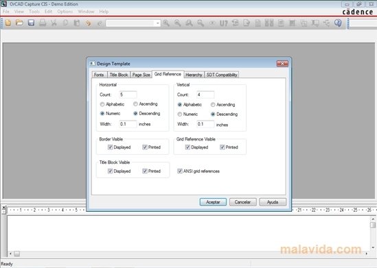
The first step to obtain one of these printed circuit boards (PCBs) is to design it using one of the specific tools on the market. One of the most popular ones is OrCAD.
OrCAD is the most powerful and intuitive tool to design printed circuit boards. The demo version offers you the possibility to evaluate the following functions: OrCAD Capture, OrCAD Capture CIS Option, PSpice A/D, PSpice A/A, OrCAD PCB Editor and SPECCTRA.
The basic steps that have to be taken to design a printed circuit board with OrCAD are:
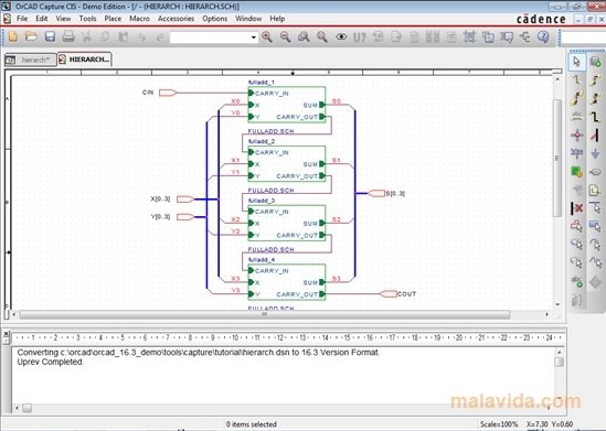
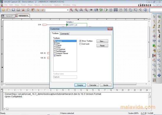
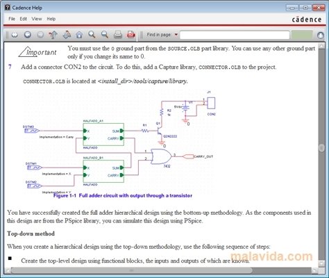
- Design the circuit by creating the schematic in the "Capture" module.
- Generate the circuit's netlist.
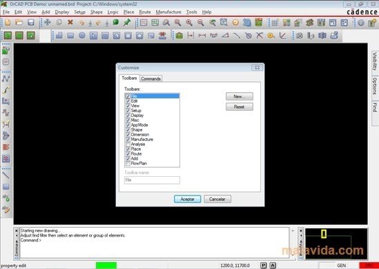
- Import the netlist to "LayoutPlus".
- Place the components and trace the pathways.
- Generate the files of its design.
Once the design of the copper pathways on the board has been finished, and we have simulated the behavior of the design, the next step will be to design the PCB from an insulating material, like for example a photosensitive fiberglass board.
 Vanessa Martín
¡Hi! I am Vanessa Martin, I like to travel, music, photography, and I am passionate about the Internet, as it is a great source of information where you can find everything you need. If it exists, it is on the Internet. Another of my great...

Antony Peel